Credit: NASA · NASA material is generally not copyrighted; items carrying a third-party or copyright credit are excluded. The NASA logo and insignia are never reused.
NASAFor more information, contact Joel W. Sills, Langley Research Center, joel.w.sills@nasa.gov.
Download PDF here
Chip resistors are widely used in NASA projects, yet cases of alumina substrate cracking during environmental testing are rare. Two instances of thick-film chip resistor cracking were observed during thermal cycling after vibration, with fractures occurring across the short axis due to bending. Failure analyses ruled out defective lots and fatigue, identifying board flexure, component orientation, excessive solder, and mounting stresses as contributing factors. The bulletin recommends careful component placement, finite element analysis, controlled solder fillet height, thorough inspection, and functional thermal shock testing to mitigate flexure-induced cracking risks in ceramic body components on printed circuit boards.
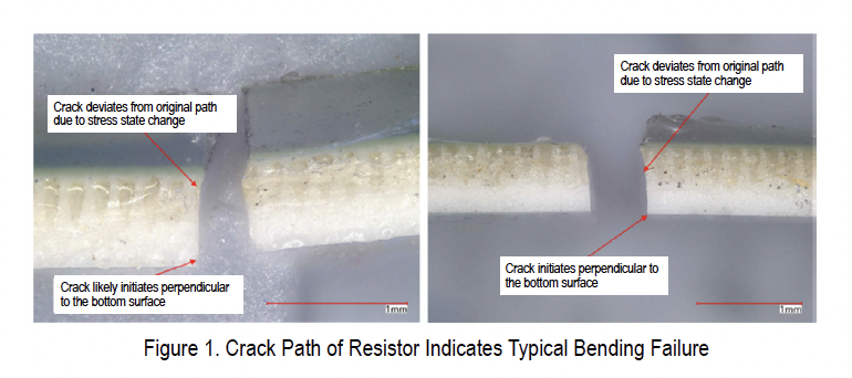
BackgroundThe NESC noted historical lack of reported cases of chip resistors’ alumina substrate cracking during vibration and thermal cycling, although chip resistors are ubiquitous across NASA projects. Two instances of thick film chip resistor body cracking were observed during environmental acceptance testing on printed circuit board assemblies. Both failures occurred during thermal cycling after vibration testing, exhibiting intermittent open circuit failures at hot dwell temperatures that recovered at room temperature. Transverse fracture occurred at the mid-span of each resistor, running parallel to the terminations. The two resistors were installed in similar locations near the edge of the boards on two identical boards. Cracks in failed resistors were along the short axis of the resistor due to apparent bending of the resistors, Figure 1. Resistors showed no signs of pre-existing defects.
Causal Relationships Initial theories pointed to vibration-induced damage of potentially defective resistors since both resistors came from the same production lot. However, the resistor lot not only meets the requirements of procurement specification MIL-PRF-55342 but additional tests were performed and did not reveal any direct evidence of a defective resistor lot. There was no evidence of an elevated risk of defective resistors within the production lot.
Failure Analyses Independent failure analyses concluded that the cracked chip resistors were due to bending/tensile failures. There was no clear-cut root cause or visible defect identifying a crack initiation site. Both resistors exhibited a single, straight crack across the short axis (perpendicular to the long axis), indicating a bending/tensile failure without twisting.
The damage signatures are not consistent with cyclic fatigue, likely ruling out fatigue failure during vibration. In addition, NESC independent optical and scanning electron microscopy (SEM), Figure 2, of both resistors did not identify any clear flaw locations for fatigue damage initiation and progression; therefore, the possibility of defective resistors as well as fatigue vibration as the root cause becomes unlikely.
Cause ConclusionsNo direct root cause was identified, but contributing factors leading to increased design consideration needed for large footprint ceramic components located near the edges of a printed circuit board that can lead to stress cracks due to manufacturing or installation bow/twist of the printed circuit board include:
Location of the relatively large resistors (case size 2512) next to the edge of the board with resistor’s long axis parallel to the card edge, increasing susceptibility to board flexure-induced damage.
Excessive solder that extended to the top pads on the resistor terminations.
Excessive bending moments or loads resulting from board bow/twist.
Hard mounting the board to a rigid frame, which can store and amplify these bow/twist stresses.
Suboptimal fastener torquing patterns, which may concentrate mounting stresses specifically at the resistor locations.
Guidelines for Assembly of Ceramic Body Components to Printed Circuit BoardsThe following guidelines are to be considered given the recent experience.
Component Orientation: Avoid orienting the long axis of large footprint ceramic components parallel to nearby printed circuit board edges to reduce susceptibility to global and local flexure damage.
Finite Element Analysis: Perform sufficient Finite Element Analysis to demonstrate adequate stress and displacement margins on large components when they must be placed near the edge of the board.
Solder Joint Fillet Limits: Keep solder off the top surface of terminations. Solder on top creates a rigid joint that transfers printed circuit board flexure directly into the ceramic increasing risk of flexure-induced cracking. Consult the individual parts manufacturers for guidance, as they may place specific limits on solder fillet height.
Solder Joint Inspection: Inspect physical solder joints or review photographic images of the joints to verify that components have sufficient, but not excessive, solder fillets according to manufacturer limits.
Functional Thermal Shock Testing: Perform one to three thermal cycles, including a hot-dwell functional test, prior to vibration testing, to document as built component integrity.
References1. MIL-PRF-55342 Resistor, Chip, Fixed, Film, Nonestablished Reliability, Established Reliability, Space Level2. MIL-PRF-55342/9 Resistor, Fixed, Film, Chip, Nonestablished Reliability, Established Reliability, Space Level, Style RM25123. MIL-STD-202 Method 218 Board Flex